This is a guide to extract the boot image from a cheap Android tablet based on Allwinner A133 using U-Boot (accessed via UART). The original firmware was not found on the internet. With the boot image and Magisk, you can root your Android tablet to make it more useful.
Pritom P7 is a very cheap Android tablet. I bought it for 33 USD from AliExpress, but it can be found for as low as 27 USD. This is a Google GMS-certified device (it passes Play Integrity, no malware was found when I received it), and it uses 32-bit Android Go. I am only using this to test some 32-bit Android app compatibility.
I bought it for 32.75 USD
They may have several variants of this model with different specifications. Mine is: Alwinner A133, 1.5GB RAM (advertised as 2GB, and shown as 2GB in the Android info), 32 GB ROM, only 2.4 GHz WIFI, no GPS.
Unlockable Bootloader
Luckily, we are allowed to unlock the bootloader of this device using the developer menu, adb reboot bootloader then using fastboot oem unlock. Some cheap Android devices don’t allow unlocking (for example, the ones that are based on recent Unisoc SOC).
I can allow bootloader unlock using the OEM Unlocking option
The product ID of my tablet is P7_EEA (Android 11) with kernel version Linux localhost 5.4.180-svn33409-ab20220924-092422 #28 SMP PREEMPT Sun Aug 20 19:13:45 CST 2023 armv8l. The build number is PRITOM_P7_EEA_20230820.
I did not find any Android exploit for this device, and I also didn’t find any backdoors. From my experience, some of these cheap Android devices have hidden su backdoors. Unable to find an exploit, I gave up trying to extract boot image from user space.
With some SOC, you can easily read/dump/extract the flash using PC software. I didn’t find any software for this Allwinner chip. An example of a SOC that allows flash reading is Unisoc (formerly Spreadtrum), but on the other hand, the bootloader on phones and tablets with the latest SOCs from Unisoc (that I know of) is not unlockable.
UART
Fortunately, this device is easy to open, and a UART pin is on the top left near the camera.
A friend gave me an Anbernic RG35XX to hack. This is a retro gaming device (it just means that it is designed to emulate old consoles). It comes with two OS: Stock OS and Garlic OS. Stock OS is closed source, and Garlic OS is open source, except for the kernel part (all are closed source). You can switch from one OS to another via a menu.
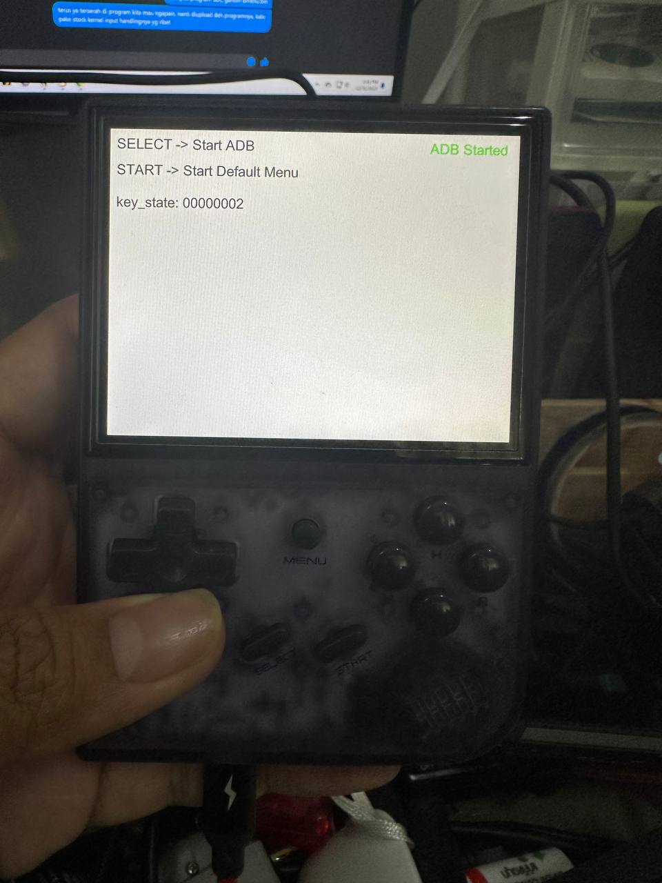
Stock OS starting my custom binary.
In my opinion, the stock OS is fast and quite user-friendly but is not customizable, although many people like Garlic OS more because it can emulate more systems.
Kernel part
Anbernic won’t release the source for ATM7039S, and no datasheet is found for this SOC. The stock RG35XX OS uses a slightly different kernel compared to the Garlic OS.
There is no serial port accessible and no debug interface available, so trying to hack the kernel will be a painful experience.
Stock RG35XX boot sequence
The kernel is stored as a uImage file on the first partition (FAT32). The built-in bootloader (u-boot) will boot load this file, and it will mount ramdisk.img. Inside ramdisk.img , we can find: /init, /init.rc, loadapp.sh. The kernel will start /init, which is based on Android init (it uses bionic libc). /init will load /init.rc, and on the last lines, it contains instructions to start loadapp.sh
service loadapp /system/bin/logwrapper /loadapp.sh
    class core
loadapp.sh will load /system/dmenu/dmenu_ln. The dmenu_ln can be found on the second partition (ext4), and this is just a shell script that will start /mnt/vendor/bin/dmenu.bin that can also be found on the second partition.
dmenu.bin is the main shell for the OS. This is written in C using SDL1.2, but it uses custom input handling instead of using SDL_WaitEvent.
Custom Input Handling
Some people swear that the input handling in the Stock RG35XX OS is faster than the other alternative OS. I can’t feel it, but the Stock OS does process input events manually.
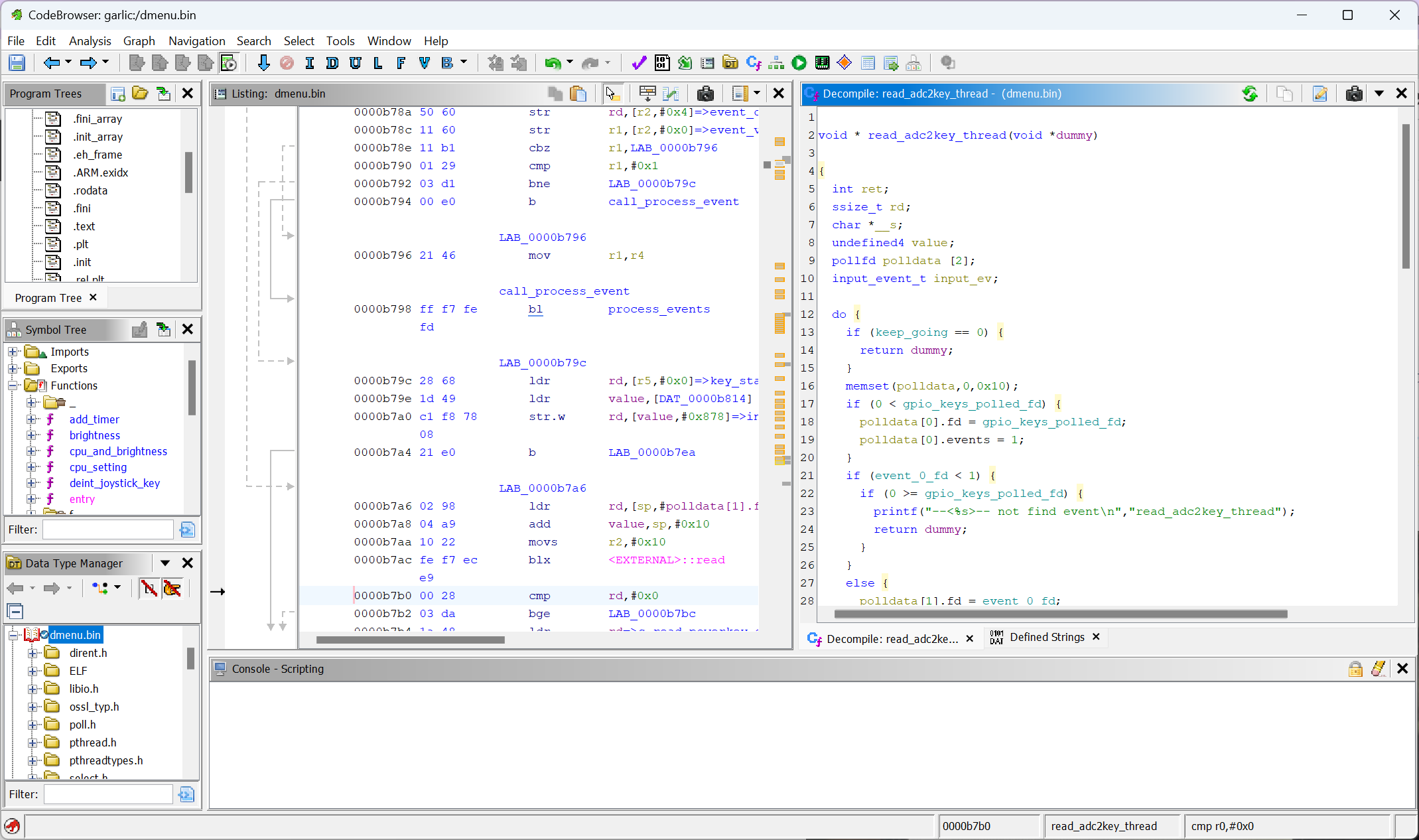
To reverse engineer how it works, I use Ghidra. Since this is not security-related software, there is no protection or obfuscation so the code can be decompiled quite cleanly.
Reverse engineering
It starts by opening /dev/input/ to find a device that has a name: gpio-keys-polled (this name is obtained using ioctl call with request EVIOCGNAME). Then, it will start a thread (using pthread) to poll this device. The power button is a separate device from all other buttons, and the reset button (under the power button) is hardwired to reset the console.
Emulator modification
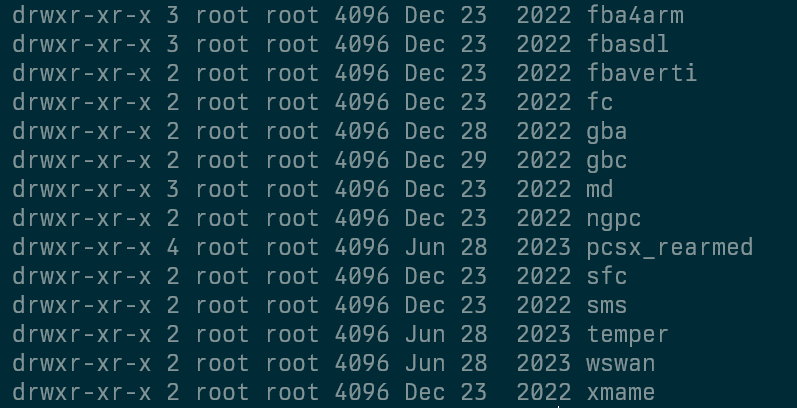
Inside appres/bin/game on the second partition, we can see several binaries for each emulator. All of them have been modified by Anbernic:
They use custom error handling
The menu button is set to display the menu (so all emulators have the same interface)
Added Video filter effect (such as dot-matrix) implemented in C (not using GPU)
Compiling for RG35XX stock OS
Usually, we will need an SDK to compile an app, but since we know the target architecture, calling convention, and the libraries used, we can work around this problem. To compile a simple SDL app that will run on the Stock OS, we will need a compiler, header files, and some libraries.
For the compiler, download Linaro toolchain 4.7 (closest to existing binaries on the system) from here (choose gnueabihf):
For the headers, download the latest SDL1.2 and use the default SDL config. And for the libraries, we can use files from /lib on the second partition. Remove libc.so and libm.so, these two are bionic files and will cause errors. Then, add files from usr/local/lib/arm-linux-gnueabihf (also from the second partition).
Then, you should be able just to compile everything manually.
Outputs to stdout/stderr will not be visible, so use dup2 to redirect these to files.
Small Demo App
In this repository, you can see my small demo app. I included all the libraries to make it easy for anyone to start (please change CC path in Makefile to your installation directory).
A bricked Xiaomi phone led me to discover a project in Github that uses a MediaTek BootROM exploit that was undocumented. The exploit was found by Xyz, and implemented by Chaosmaster. The initial exploit was already available for quite a while. Since I have managed to revive my phone, I am documenting my journey to revive it and also explains how the exploit works. This exploit allows unsigned code execution, which in turn allows us to read/write any data from our phone.
For professionals: you can just skip to how the BootROM exploit works (spoiler: it is very simple). This guide will try to guide beginners so they can add support for their own phones. I want to show everything but it will violate MediaTek copyright, so I will only snippets of decompilation of the boot ROM.
Bricking my Phone and understanding SP Flash Tool
I like to use Xiaomi phones because it’s relatively cheap, has an easy way to unlock the bootloader, and the phone is easy to find here in Thailand. With an unlocked bootloader, I have never got into an unrecoverable boot loop, because I can usually boot into fastboot mode and just reflash with the original ROM. I usually buy a phone with Qualcomm SOC, but this time I bought Redmi 10X Pro 5G with MediaTek SOC (MT6873 also known as Dimensity 800). But it turns out: you can get bricked without the possibility to enter fastboot mode.
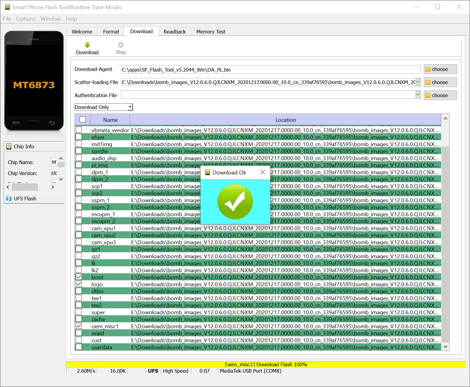
A few years ago, it was easy to reflash a Mediatek phone: enter BROM mode (usually by holding the volume up button and plugging the USB when the phone is off), and use SP Flash Tool to overwrite everything (including boot/recovery partition). It works this way: we enter BROM mode, the SP Flash Tool will upload DA (download agent) to the phone, and SP Flash Tool will communicate with the DA to perform actions (erase flash, format data, write data, etc).
But they have added more security now: when I tried flashing my phone, it displays an authentication dialog. It turns out that this is not your ordinary Mi Account dialog, but you need to be an Authorized Mi Account holder (usually from a service center). It turns out that just flashing a Mediatek phone may enter a boot loop without the possibility of entering fastboot mode. Quoting from an XDA article:
The developers who have been developing for the Redmi Note 8 Pro have found that the device tends to get bricked for a fair few reasons. Some have had their phone bricked when they were flashing to the recovery partition from within the recovery, while others have found that installing a stock ROM through fastboot on an unlocked bootloader also bricks the device
I found one of the ROM modders that had to deal with a shady person on the Internet using remote Team Viewer to revive his phone. He has some explanation about the MTK BootROM security. To summarize: BROM can have SLA (Serial Link Authorization), DAA (Download Agent Authorization), or both. SLA prevents loading DA if we are not authorized. And DA can present another type of authentication. Using custom DA, we can bypass the DA security, assuming we can bypass SLA to allow loading the DA.
When I read those article I decided to give up. I was ready to let go of my data.
MTK Bypass
By a stroke of luck, I found a bypass for various MTK devices was published just two days after I bricked my Phone. Unfortunately: MT6873 is not yet supported. To support a device, you just need to edit one file (device.c), which contains some addresses. Some of these addresses can be found from external sources (such as from the published Linux kernel for that SOC), but most can’t be found without access to the BootROM itself. I tried reading as much as possible about the BROM protocol. Some of the documentation that I found:
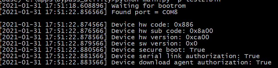
Another luck came in a few days later: Chaosmaster published a generic payload to dump the BootROM. I got lucky: the generic payload works immediately on the first try on my phone and I got my Boot ROM dump. Now we need to figure out what addresses to fill in. At this point, I don’t have another ROM to compare, so I need to be clever in figuring out these addresses. We need to find the following:
send_usb_response
usbdl_put_dword
usbdl_put_data
usbdl_get_data
uart_reg0
uart_reg1
sla_passed
skip_auth_1
skip_auth_2
From the main file that uses those addresses we can see that:
uart_reg0 and uart_reg1 are required for proper handshake to work. These addresses can be found on public Linux kernel sources.
usbdl_put_dword and usbdl_put_data is used to send data to our computer
usbdl_get_data is used to read data from computer
sla_passed, skip_auth_1 and skip_auth_2, are the main variables that we need to overwrite so we can bypass the authentication
We can start disassembling the firmware that we obtain fro the generic dumper. We need to load this to address 0x0. Not many strings are available to cross-reference so we need to get creative.
Somehow generic_dump_payload can find the address for usb_put_data to send dumped bytes to the Python script. How does it know that? The source for generic_dump_payload is is available in ChaosMaster’s repository. But I didn’t find that information sooner so I just disassembled the file. This is a small binary, so we can reverse engineer it easily using binary ninja. It turns out that it does some pattern matching to find the prolog of the function: 2d e9 f8 4f 80 46 8a 46. Actually, it searches for the second function that has that prolog.
Pattern finder in generic_dump_payload
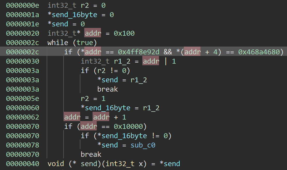
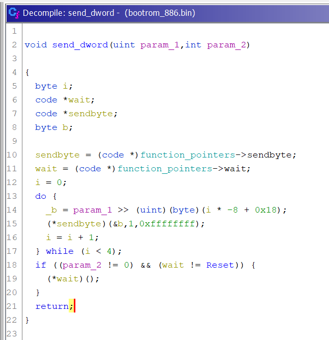
Now that we find the send_word function we can see how sending works. It turns out that it sends a 32-bit value by sending it one byte at a time. Note: I tried continuing with Binary Ninja, but it was not easy to find cross-references to memory addresses on a raw binary, so I switched to Ghidra. After cleaning up the code a bit, it will look something like this:
What generic_dump_payload found
Now we just need to find the reference to function_pointers and we can find the real address for sendbyte. By looking at related functions I was able to find the addresses for: usbdl_put_dword, usbdl_put_data, usbdl_get_data. Note that the exploit can be simplified a bit, by replacing usbdl_put_dword by a call to usbdl_put_data so we get 1 less address to worry about.
The hardest part for me was to find send_usb_response to prevent a timeout. From the main file, I know that it takes 3 numeric parameters (not pointers), and this must be called somewhere before we send data via USB. This narrows it down quite a lot and I can find the correct function.
Now to the global variables: sla_passed, skip_auth_1, and skip_auth_2. When we look at the main exploit in Python, one of the first things that it does is to read the status of the current configuration. This is done by doing a handshake then retrieve the target config.
Target config
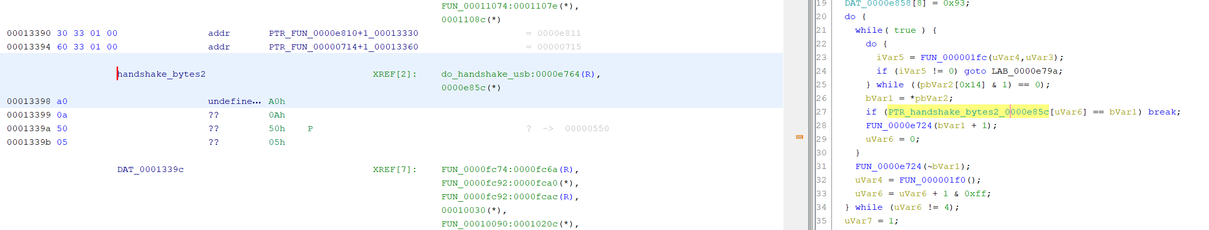
There must be a big “switch” statement in the boot ROM that handles all of these commands. We can find the handshake bytes (A0 0A 50 05) to find the reference to the handshake routine (actually found two of them, one for USB and one for UART). From there we can find the reference to the big switch statement.
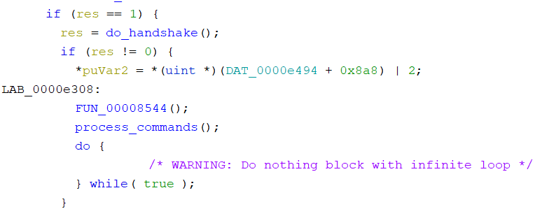
The handshake
You should be able to find something like this: after handshake it starts to handle commands
And the big switch should be clearly visible.
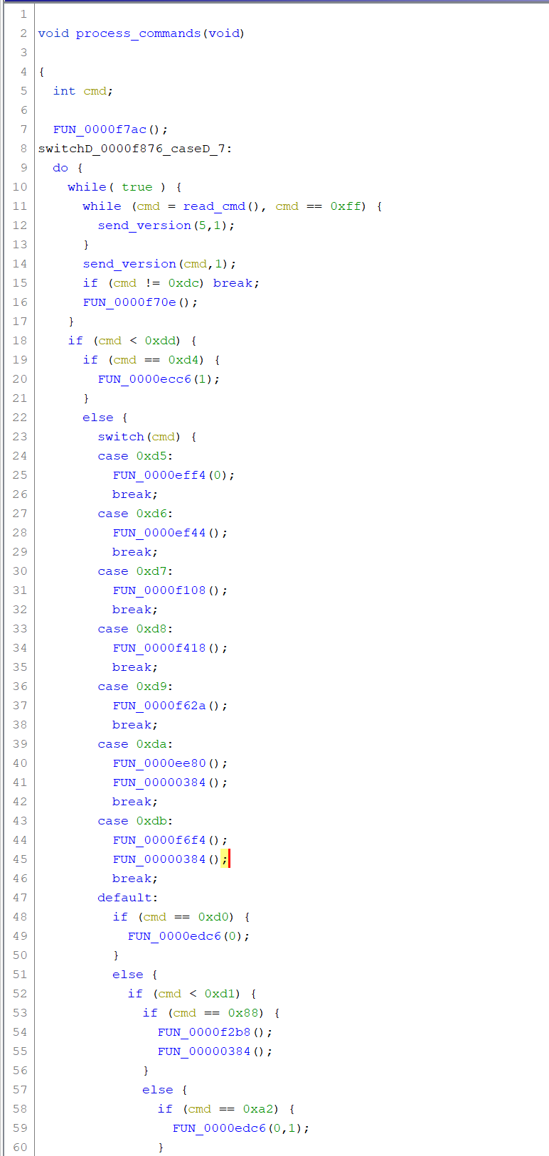
Switch to handle various commands
Now that we found the switch, we can find the handler for command 0xd8 (get target config). Notice in python, the code is like this:
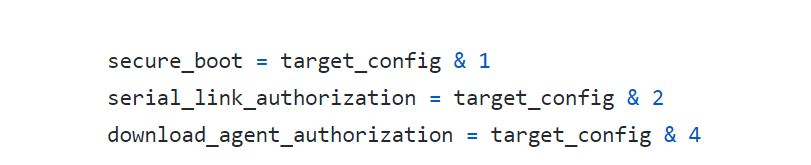
Notice the bit mask
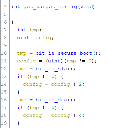
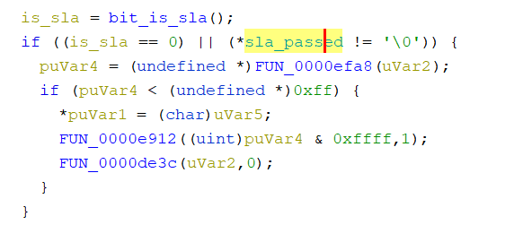
By looking at the bitmask, we can conclude the name of the functions that construct the value of the config. E.g: we can name the function that sets the secure boot to is bit_is_secure_boot. Knowing this, we can inspect each bit_is_sla and bit_is_daa
we can name the functions from the bit that it sets
For SLA: we need to find cross-references that call bit_is_sla, and we can see that another variable is always consulted. If SLA is not set, or SLA is already passed, we are allowed to perform the next action.
finding sla_passed
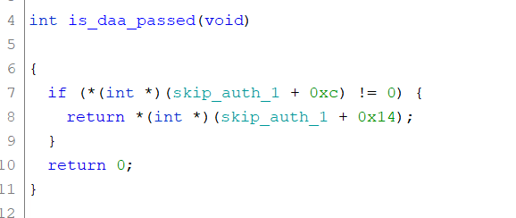
Now we need to find two more variables for passing DAA. Looking at bit_is_daa, we found that at the end of this function, it calls a routine that checks if we have passed it. These are the last two variables that we are looking for.
How the BootROM Exploit Works
The exploit turns out very simple.
We are allowed to upload data to a certain memory space
Basically it something like this: handler_array[value*13]();
But there are actually some problems:
The value for this array is unknown, but we know that most devices will have 0x100a00 as one of the elements
We can brute force the value for USB control transfer to invoke the payload
We may also need to experiment with different addresses (since not all device has 0x100a00 as an element that can be used)
Another payload is also provided to just restart the device. This will make it easy to find the correct address and control value.
Closing Remarks
Although I was very upset when my phone got bricked, the experience in solving this problem has been very exciting. Thank you to Xyz for finding this exploit, and ChaosMaster for implementing it, simplifying it, and also for answering my questions and reviewing this post.
It has been almost 6 months since I published my Pokemon Go Plus finding and so far no one has published their Pokemon Go Plus Key. One of the reason is the difficulty in extracting the key from OTP (one time programmable) memory that requires precision soldering. Few weeks after I wrote my article, I posted an idea to /r/pokemongodev to extract a Pokemon Go Plus key using over the air (OTA) update.
The idea was based on two things:
We can flash any image using SPI Flasher, and there is no signature check, we just need a correct checksum.
The SPI flash contains two copies of the same firmware (there are 2 firmware banks). This is important for OTA: in case the firmware was not transferred correctly, the bootloader (located in OTP) will boot the other valid firmware
And the plan was this:
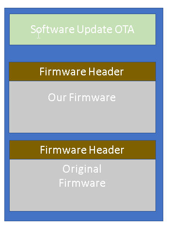
Create our new custom firmware
Flash the new firmware to the Pokemon Go Plus over the air to Bank 1. At this point there will be two firmware: our firmware and the pokemon go plus firmware
Extract the key via BLE (Bluetooth Low Energy) using the new firmware
Restore the original firmware by sending a special request to the new firmware. This is done by reading the original firmware on bank 2 and overwriting our firmware in Bank 1.
The plan
Unfortunately, I don’t have time to implement it. I don’t have DA14580 development board so I won’t be able to debug it properly via JTAG. I don’t feel like buying 40 USD for a board that I will only use for this project. I got about 30 USD in donations which I use to buy another Pokemon Go Plus clone, it has the same Bluetooth MAC address. (Note that money wasn’t really the problem, I just like to spend it on something that I like, for example, I just recently bought Nvidia Jetson Nano and a Stereo Microscope)
Two months ago a Reddit user jesus-bamford contacted me, mentioning that he will implement the idea I proposed. Everything seems to work according to plan:
He can create a firmware that can extract the key from OTP
He can write his firmware using SPI flasher
He can send his firmware over the air (using Android App provided by Dialog Semiconductor)
But this is where the good news ends: if the firmware is written using OTA, it won’t boot. The bootloader thinks the firmware is invalid and it will boot the original copy of the Pokemon Go Plus firmware. He found out that there is an extra check in the Software Update that was added, that is not in the source code provided in the DA14580 SDK. But he can’t figure out what is the check or how to bypass it.
During the Songkran Holiday in Thailand, I have some free time so I tried to reverse engineer the boot loader. He is right, there is an extra check added:
When the update process is started, a flag is set to indicate that this firmware image is not yet valid. In case of a failed update, the bootloader can bot the other valid firmware. During this process, an SHA256 hash is initialized
For every incoming data that is written to SPI flash, the hash is updated
At the end of the update, a signature check is performed based on the SHA256 AND some data from OTP. If everything is valid, then the firmware image is set to valid.
I didn’t go into detail on the signature check algorithm, I know it uses big number computations, probably RSA but I didn’t verify it. I also don’t feel that I will find a bug there. What’s important is what happens next: if the signature is valid then a flag is set to indicate that the image is valid.
So to be clear:
If we modify a firmware using SPI flasher, we just overwrite existing firmware and the valid flag is kept on
If we modify a firmware using OTA, we need it to be set as valid at the end of the update process
I know one thing for sure: the update process also requires a specific key from the OTP area. So if there was ever going to be an update from Niantic, that update requires a connection to their server to get a special key from them.
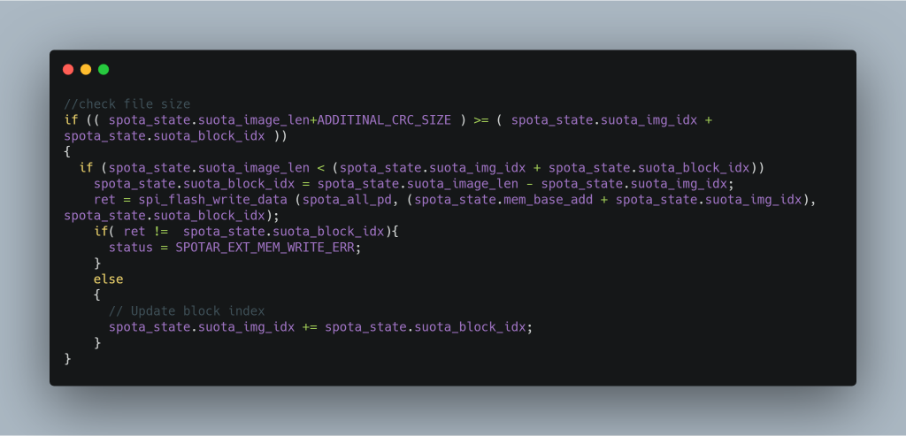
So let’s go back and see if there is another way to set the image to be valid. This is the original source code inside app_spotar_img_hdlr.c in the DA14580 SDK:
The compiled binary has an extra call to update the SHA256, but its not important for now. Lets focus on just this one line:
ret = spi_flash_write_data (spota_all_pd, (spota_state.mem_base_add + spota_state.suota_img_idx), spota_state.suota_block_idx);
The variable spota_all_pd contains data sent from the updater app. The second parameter specifies where to write the data (the address in SPI block) and the third parameter is the size.
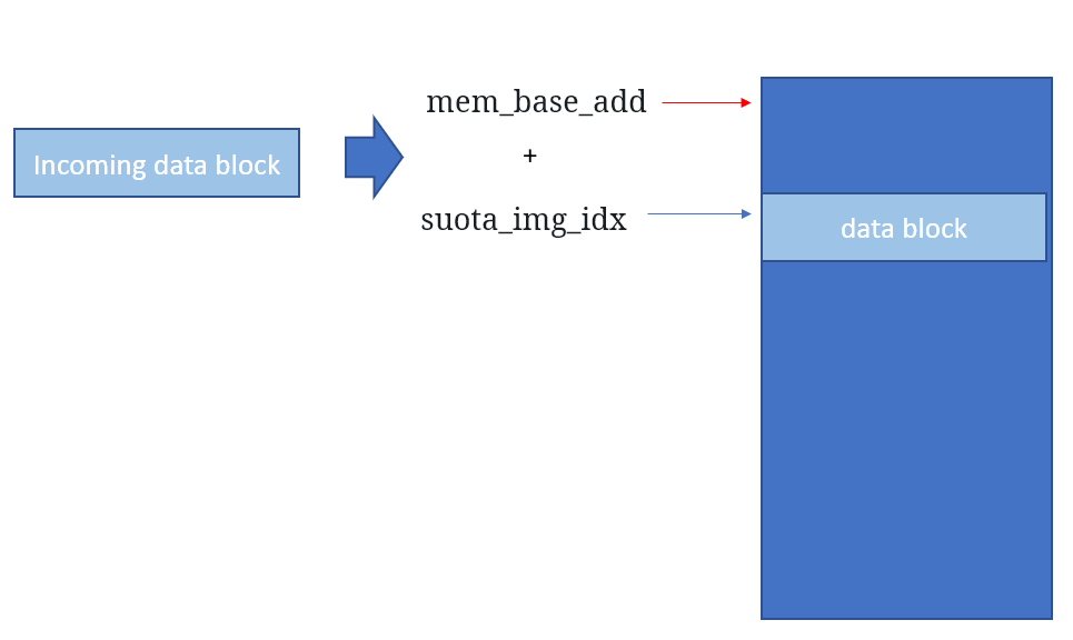
Visually, we can see that mem_base_add points to the beginning address in the SPI flash, and suota_img_idx points to the current block.
When the write is succesful we increment the address through:
It seems to be fine. I looked for possible buffer overflows for code execution and I couldn’t find one. But what if we can modify spota_state.mem_base_add then we will be able to write anywhere in the SPI flash, including in the image valid flag.
I found a function called: app_spotar_read_mem which is supposed to be called after we finished writing all of the data. This is also where the final check is performed before writing,
This code is very strange: instead of using a temporary variable it uses: spota_state.mem_base_add to store a temporary value to be used for setting spota_state.suota_image_bank. When spota_state.mem_base_add is greater than 2 this function will fail.
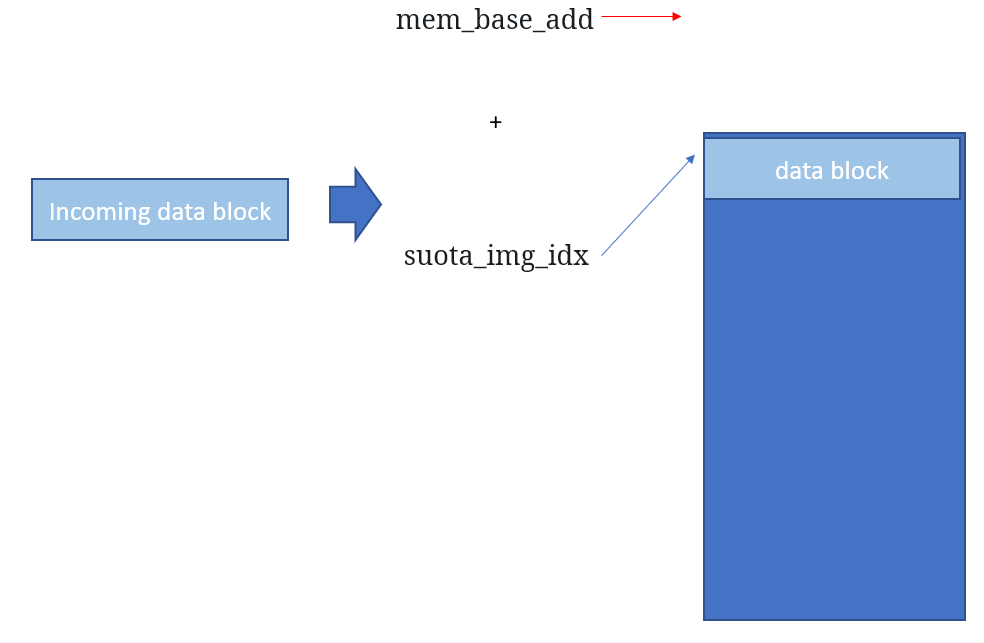
And this is exactly what we need: a way to modify mem_base_add. So what we need to do is:
Send data via OTA as usual, and this will be written to SPI as expected
Before sending the last part of the data, send a request such that app_spotar_read_mem is called, and set the mem_base_add to the beginning of our firmware header, where the valid flag is
Send the last part of the data, which will overwrite the firmware header. This last data is the header that we want
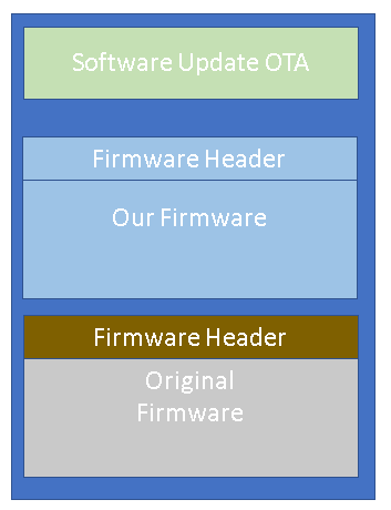
Moving mem_base_add up
And that’s the idea. Jesus-bamford did a great job implementing this idea and I was so happy that it works. Here is his software in action. The firmware is already open source at:
But the updater is not yet ready for release. He is currently reimplementing the OTA software for Android because his current code is based on the SDK code. When he is finished, anyone should be able to extract their Pokemon Go Plus key without opening it.
I know that I should probably wait until his work is finished before publishing this, but I am also hoping that others can help him. May be implement the update for different iOS, or start working on implementation of Pokemon Go Plus for other devices.
It might also be possible to implement the Pokemon Go Plus using EdXposed (this is a fork of XPosed that works with Pokemon Go) or by adding a library to the iOS version that intercepts the BLE API calls.
TL;DR; You can clone a Pokemon GO Plus device that you own. I have managed to get the certification algorithm. However, there is a per device blob used (specific to a Bluetooth Mac Address) for key generation. I have not figured out how you can generate your own blob and key. Using other’s people blob may be blacklisted in the future (or Niantic may ban your account).
Pokemon GO Plus, (which I will refer from now on as PGP) is a wearable Bluetooth Low Energy (BLE) device to be used with the Pokemon GO game for Android or iOS. There have been many attempts to clone this device, but only Datel seems to figure out the algorithm, while the other clones are cloning the exact hardware and firmware.
I will explain the complete certification algorithm that I obtain from reverse engineering a PGP clone, and then I will explain how I did the reverse engineering and how you can extract your own blob and key if you want to clone your own device. I am providing a reference implementation for ESP32 so you can test this yourself, the source code DOES NOT INCLUDE the BLOB and DEVICE KEY.
Before I begin, let me start with the current state of Pokemon GO Reverse and PGP reverse engineering.
A short history of past reverse engineering attempts
I am writing this to clear up some confusion that people have on the current state of Pokemon GO Game/App and PGP reverse engineering. The first few versions of Pokemon GO were not protected at all. In a short amount of time people were making bots and maps. Then things changed when Niantic implemented a complex hashing algorithm for the requests to their servers, but this too was quickly defeated with collaboration from many hackers.
Starting from version 0.37 on around second week of September 2016 (which is the first version that supports PGP), Niantic added a very complex obfuscation to the native code, and since then they have changed the hashing method several times, and lately also added encryption. Since the obfuscated version came out, only a few people worked on cracking the new algorithms. For a while, there was a group that runs a hashing-as-a-service with a paid subscription but since a few months ago they haven’t reopened their service. Either they have not figured out the latest protection or may be catching up with Niantic is getting boring or no that profitable.
On the PGP side, ever since this device was announced in 2016, many have tried to reimplement it in some form of hardware (for example this). Before the device was announced, the Pokemon GO app was still not obfuscated and the certification algorithm was not included yet. When the PGP device was finally released, the corresponding Pokemon GO app that supports it was already obfuscated.
On January 2017, a Reddit user BobThePigeon_ wrote a quite detailed article about reverse engineering PGP device. He figured out part of the certification process, but it turns out that it was not the complete process (this is the reconnection protocol). The certification is done at first connection which generates a key to be used at subsequent connections. His write-up only covers the reconnection part. Unfortunately, he didn’t continue this effort, and he never posted anything related to this. So currently (until now) there is no open source PGP device available since the device release data in 2016.
Even though no one has published the certification algorithm, Datel/Codejunkies has managed to reverse engineer this and released their clone: Gotcha and Gotcha Ranger. Just for your information, this company has been in this reverse engineering business for a few decades.
PGP BLE Peripheral
This background information is needed to understand the certification algorithm. PGP is a BLE peripheral that provides three services:
Battery Level (a standard service)
LED and button (a custom service)
Certification (a custom service)
To be recognized by Pokemon Go app/game, it needs to announce its name as: “Pokemon GO Plus”, “Pokemon PBP”, or “EbisuEbisu test”.
Before the LED and Button can be used, we need to pass the certification process. There are three characteristics (“characteristics” is a BLE term) provided by the certification service:
SFIDA_COMMANDS (for notifying the game to continue to the next step)
CENTRAL_TO_SFIDA (for sending data to PGP)
SFIDA_TO_CENTRAL (for reading data from PGP)
The flow of data is:
The app can write anytime to CENTRAL_TO_SFIDA
When PGP needs to send something, it sets the SFIDA_TO_CENTRAL characteristic value and notifies the app using SFIDA_COMMANDS notification
The app can read anytime from SFIDA_TO_CENTRAL
I will not go into detail about the other two services:
The battery service must exist because the app reads it
Someone already reversed engineered the LED pattern, so I wont go into detail about this
Certification Algorithm
Several people have tried reverse engineering based on the Bluetooth Low Energy (LE) traffic but were unable to get the detail of the certification algorithm. This is because the protocol uses AES encryption with a key that is not in the transferred data (so protocol analysis based on traffic alone is not possible).
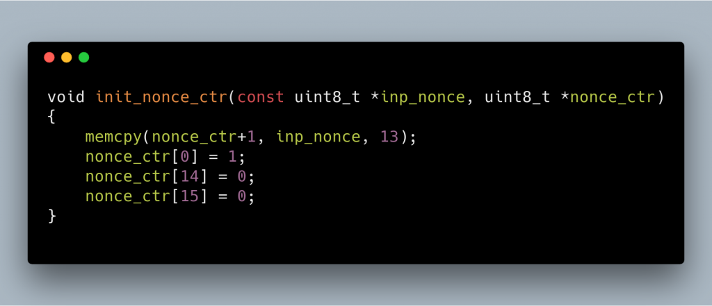
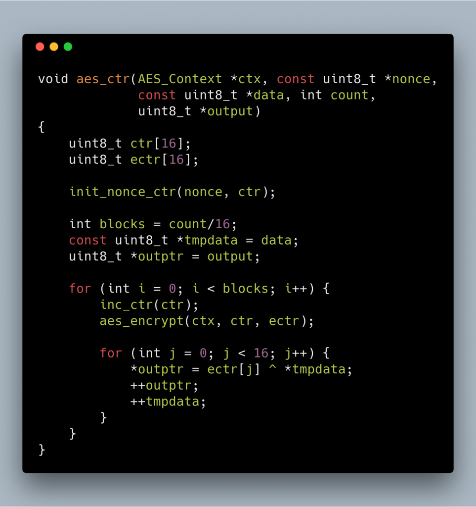
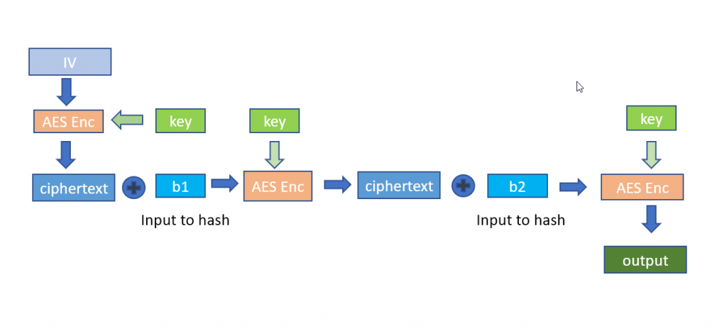
First I will describe three special functions needed by the protocol. The first one is AES CTR. This is the same as normal AES CTR, except for the counter initialization and the increment function.
Please note that when exchanging nonce we exchange 16 bytes, only 13 bytes are used, and the other 3 bytes are overwritten. The nonce for AES CTR is prepared as pictured: first byte, and last two bytes are set to 0, and we copy the 13 bytes of the nonce (starting from offset 0) to offset 1 in the nonce.
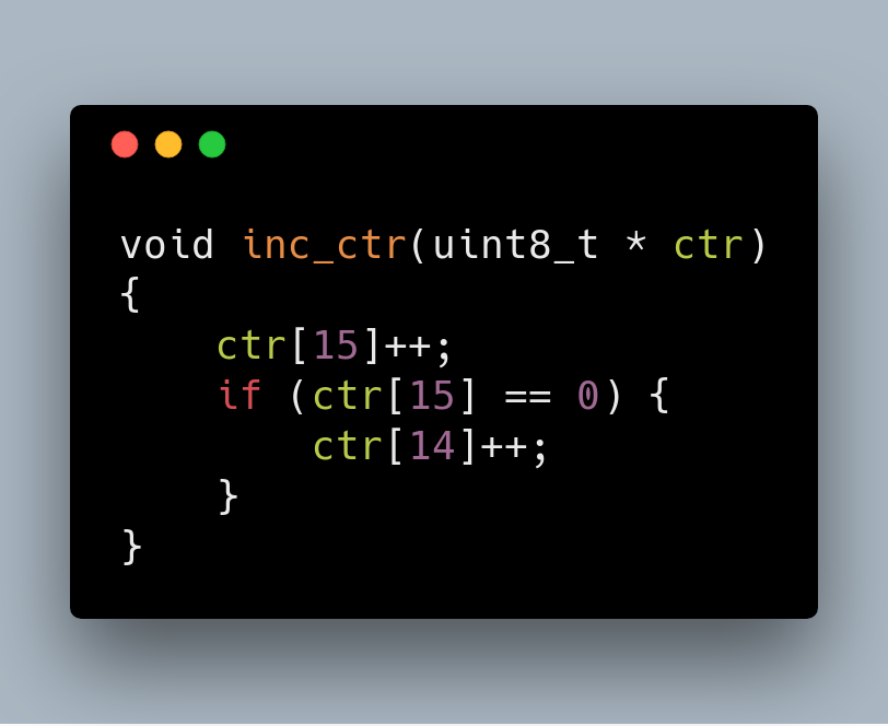
To increment the nonce, we increment the last byte (offset 15), and when it becomes 0, we increment the previous byte (offset 14)
And this is how the AES-CTR is implemented
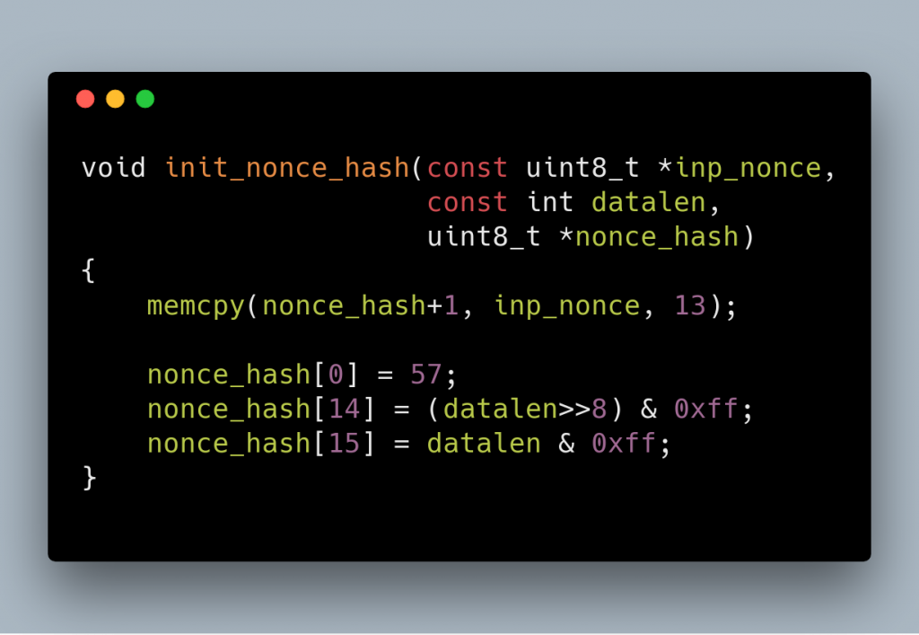
The second one I named it AES Hash, which uses AES to create a 128 bit hash from data. This one requires another nonce which is derived from nonce. This time we set the first byte to 57, and the last 2 bytes to the size of the data to hash.
And here is the hash algorithm. This just encrypts the nonce, then xor it with each block of input data, then encrypt again.
And the code is as follows
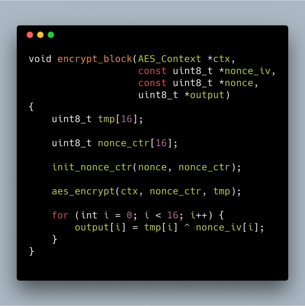
The third one is Encrypt Block which encrypts a nonce that is initialized as if it is going to be used in AES-CTR, then xors it with a data.
Now we can discuss the protocol.
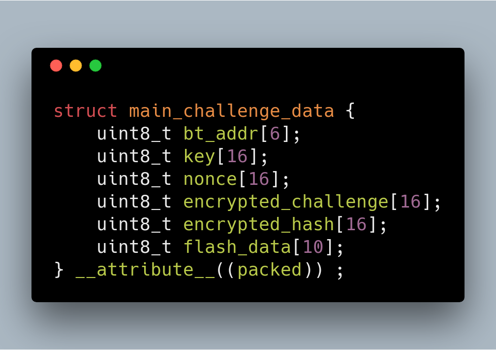
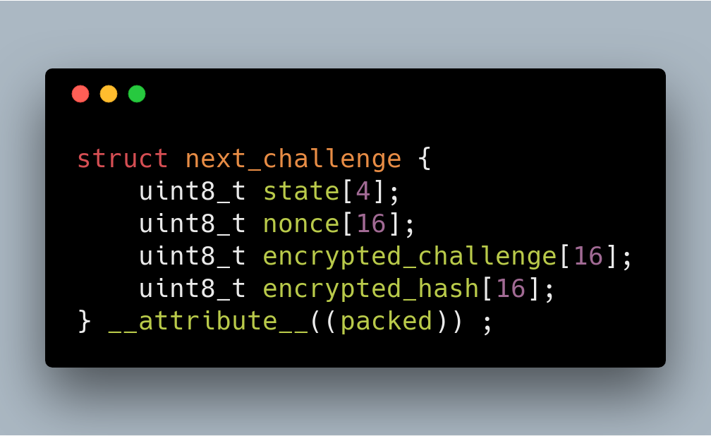
PGP will generate a random 16 bytes challenge (A), a random 16 bytes session key (Sk), and a random 16 bytes nonce (N1). Encrypt A using Sk . This key, encrypted data, encrypted hash and nonce along with Bluetooth address (in reversed order) and some data obtained from the SPI flash (in my case it is always all 0) is then packed in the structure pictured below.
The content of encrypted_challenge is the output of aes_ctr. The content of encrypted_hash is result of aes_hash encrypted with encrypt_block. This explanation also applies to next parts wherever we have “encrypted_challenge” and “encrypted_hash”.
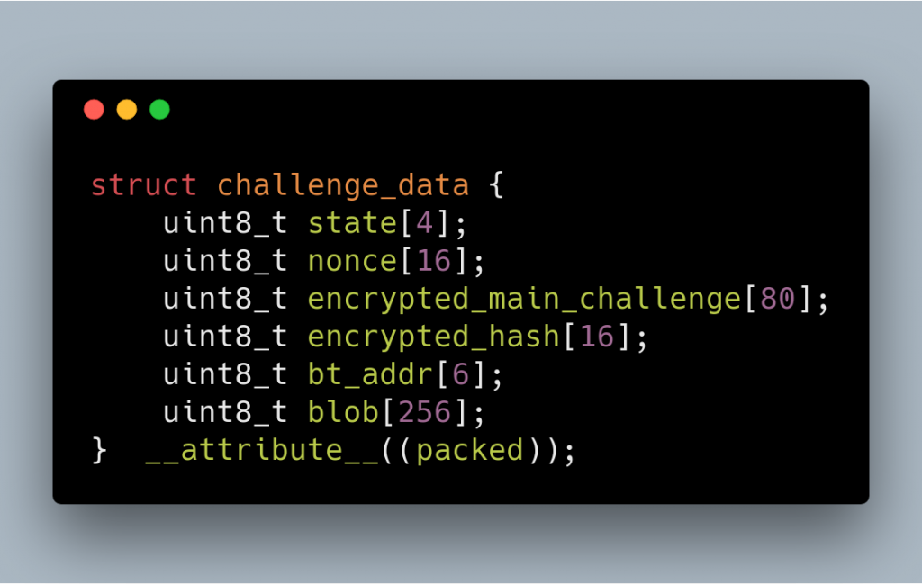
The 80 bytes is then encrypted using a “device key” which is dependent on the device. PGP prepares 378 bytes of data, consisting of:
State (always 00 00 00 00)
The encrypted main_challenge_data (80 bytes)
A nonce (this nonce can be different from the nonce inside main_challenge_data)
The encrypted hash
Bluetooth Mac address (this is also on the encrypted main_challenge_data)
256 bytes of data blob from OTP (one-time programmable memory)
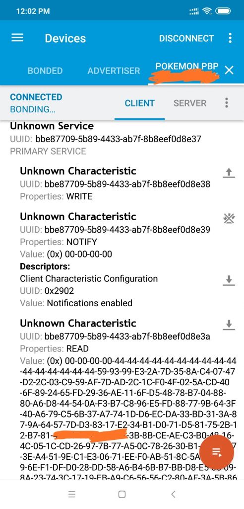
When Pokemon GO App connects to PGP, PGP will prepare the challenge data, then signals the Pokemon Go app to read the data. The Pokemon Go app knowing the “device key” will be able to extract the challenge A and sends back A , with prefix 00 00 00 00 to PGP.
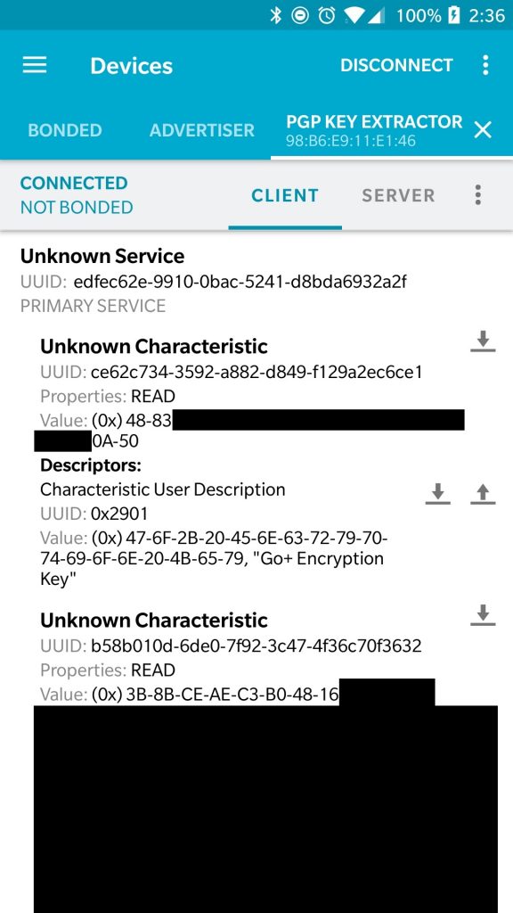
Viewing challenge data using nRF Connect app
PGP will check that the 16 bytes (A) are indeed the same as the one that was sent. If not then it will terminate the connection. In general, in any step, if something is not right, the connection will be terminated.
For the next few steps, the challenge will have the following format (size of this is 52 bytes).
PGP will encrypt this static data: 0xaa followed by 15 bytes of NULs (0x00), using the session key (Sk), sets the state to 01 00 00 00 and notify the app to read the data.
The app will decrypt the data, and check if the decrypted data is 0xaa followed by 15 zeroes. If it is as expected, the app will generate random 16 bytes data, encrypts it and pack it in the same format. Note that in BLE world, app payload packet is limited to 20 bytes, so this will come in several packets.
PGP now needs to decrypt this data, and prepare a buffer prefixed by 02 00 00 00 and notify the app to read it. This proves to the app that the PGP device can decrypt the data from the app.
The app will send 52 bytes of data (again according to the next_challenge structure) then PGP will just notify with the value: 04 00 23 00, signaling that everything is OK. When decrypted this final challenge contains the string “PokemonGoooooooo”. The app will then subscribe to button notifications and will start writing to LED characteristics when it finds a Pokemon or a Poke gym.
At this point, the green color should light up on the PGP icon.
We can tap on the green icon, and the app will disconnect from the PGP. We can tap it again to reconnect. At this point, we can just forget about everything and starts the protocol from the beginning again, or we can perform a reconnection protocol which is faster. This reconnection protocol is the one that is explained by BobThePigeon_.
For this reconnection, we will use the session_key (Sk) that we use in the previous exchange. PGP will generate two 16 bytes random value (let’s call them A and B), and expects the App to respond with:
AES_ENCRYPT(session_key, A) xor B
After PGP verifies that it is correct, the app will then send another two 16 bytes random (let’s call them C and D), and expects PGP to respond with:
AES_ENCRYPT(session_key, C) xor D
When the app verifies that everything is fine, it will send 03 00 00 00 01, and PGP will then acknowledges by notifying the value: 04 00 02 00.
LED, Vibration and Button
When we encounter a Pokemon or Pokestop, the app will send a pattern of lights to be played by PGP. The app will then read the button status to decide what to do with the information. So we can’t reprogram it to select a particular ball or to give berries.
Because other people have explained this better than me, I will not repeat it again. Here is a good explanation from a Reddit user on this thread.
The next logical step after understanding the process is to reimplement this algorithm in a new hardware to test that it is indeed correct. I started with Android (turns out to be almost impossible), then Raspberry Pi Zero W (got stuck on some bluez stuff), and finally resorts to ESP32.
Android BLE peripheral emulation
At first, I thought that this is the best method: anyone that has a spare Android can test this. It turns out to be not easy: Android can act as a BLE peripheral but will randomize its MAC address on every announcement. This is done for privacy reason but I thought that it will make it impossible to implement PGP emulation because the PGP protocol uses Mac Address in the encryption process.
It turns out that on iOS, the app can’t get BLE address of the peripheral, so I (or someone) should try again reimplementing this in Android. For the Android game version: Niantic should be able to detect/block this easily.
Pi Zero W peripheral emulation
The next arsenal that I have is a Raspberry Pi Zero W. I have checked that it is possible to do peripheral emulation using bluez, and it is also possible to change the mac address for BLE. It is also possible to program this using Python, so it seems to be a good choice.
However, I was stuck with the bluez/dbus API. The documentation is quite sparse. So I gave up with Pi Zero W. I think it should be possible to do this in Pi Zero W. I don’t want to spend a lot of time debugging the bluez stack so I switched to something that is easier to debug.
ESP32
I chose this device because this device is very cheap (the cheapest is around 5 USD delivered), is easy to program, and I happen to have a few of them. I didn’t have any experience before in programming BLE for ESP32, but programming BLE in this platform is very straightforward. Please note that I just copied and modified the examples provided in the esp-idf , so what I did may not be the most correct or efficient way to do it.
I also provided Makefile.test which can be used on the desktop to test the encryption algorihtms, just run make -f Makefile.test and run cert-test.
This app doesn’t have a visual indicator, after flashing with “make flash”, run “make monitor” to see pairing progress. Press “q” to simulate button press and “w” to clear button press notification (although this doesn’t seem to be necessary).
I didn’t test the implementation for an extended amount of time. I only tested the following:
It can be paired, disconnected, reconnected
It can receive notifications when there are Pokemon around me
It can send button press (using ‘q’ key in the serial monitor) to catch the Pokemon
You will need the following data from the device that you clone:
Bluetooth MAC address (easily extracted using Bluetooth connection)
Fixed data (easily extracted using Bluetooth connection)
device key (currently requires soldering)
You can read the method to extract the device key on the next part.
Reversing PGP
This is the details of the reverse engineering part. This part is divided into two main parts: the hardware reversing and firmware reversing.
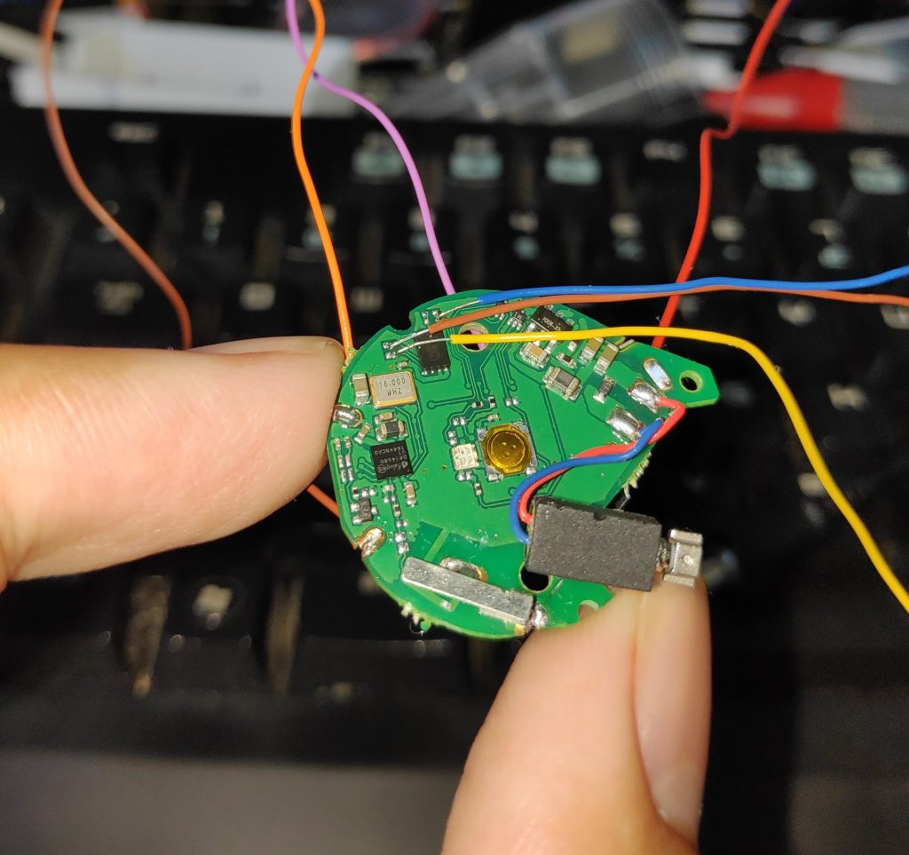
The hardware
I bought a Chinese clone of the PGP for about $20 including shipping (the original one would cost me $88 including shipping to Thailand)., and when I opened the PGP, it turns out the be an exact clone of the original. It uses the same DA14580 chip with the same PCB layout.
Fortunately, this one is a bit easier to solder due to the solder pads that exists in the cloned version.
This is the clone device that I have, same MCU, same PCB layout, same firmware as the original
I used a $5 USB Soldering iron with a wrapping wire and it works quite OK. I was a bit amazed that the everything works on the first try.
$5 Soldering iron
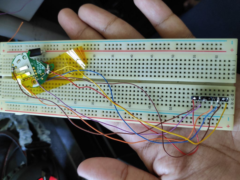
I held the board in place with Kapton tape on a breadboard.
Since the hardware is the same, I tried following what BobThePigeon_ already did: holding the RST and read the flash. I use the flashrom package on Raspberry Pi software to read the SPI flash (you can also use Arduino board, Bus Pirate, or anything that can read SPI Flash).
Later on I also made a code to patch and reencrypt the firmware which can be uploaded using the same SPI connection.
After extracting it and comparing the description with his write-up, it turns out to be using the exact same firmware as described by BobThePigeon_. So all the AES keys that encrypt the firmware is also the same. It also means that when there is a new update for PGP, this device should also be updateable.
For the hardware debugging, I did not use JTAG to debug the firmware. I did not perform a dynamic analysis using a debugger. So basically I only used a few cables to read and write the SPI flash.
Deeper into the firmware code
BobThePideon_ wrote that “All this information is in Dialog Semiconductor’s DA14580 SDK, however, you have to jump through some hoops to get the SDK.“. Well, it turns out getting the SDK is quite an easy process, and having the SDK helps a lot in understanding the firmware. Even though I don’t have a DA14580 devkit board, I can try to compile and see what the resulting code will look like.
The main firmware is 31984 bytes long and since this is Cortex-M0, it uses Thumb instruction set. This firmware is loaded at starting memory location: 0x20000000. It is not easy to understand the code just by looking the code in a disassembler, so my first approach is to try to see what a real firmware would look like if it has a full debugging information.
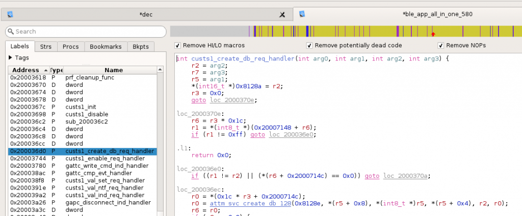
After installing the DA1458x_SDK and Keil uVision5 we can compile the examples (for instance ble_app_all_in_one). My first thought was to generate assembly code from C file (like the -S option in gcc), but this is not allowed in the free version of Keil uVision. But we have the next best thing: an ELF with debugging symbol. On the output folder, I saw an AXF file, which is actually an ELF file with debug information. This helps a lot in understanding a firmware designed for DA14580.
Opening AXF file, this is much easier to understand
Now we can see clearly how the code calls ROM functions which is located from 0x20000-0x35000, and I can understand the mapping in rom_symdef.txt file:
sdk/common_project_files/misc/rom_symdef.txt
For example, in the PGP firmware, the function at the address 20006e24 just calls 0x33b21 which according to the rom_symdef.txt is __aeabi_memcpy. Renaming these procedure is like finding the edges of a puzzle.
I spent quite a lot of time looking at SDK to understand more about its structure, convention, and constants that might help.
Inside platform\core_modules\rwip\api\rwip_config.h we can see the standard TASK number (for example for battery service, firmware update service, etc). This task numbers also helps identify different subroutines that call ke_msg_alloc, by convention, the ID of the message is: TASK_ID << 10 + message
Some interesting subroutine/function locations:
At address 0x20005758 is the function that copies data from OTP (blob and device key)
At address 0x200065DC is the main AES encryption (also the read AES implementation in sdk/platform/core_modules/crypto/), by finding cross-reference to this, we can get the subroutine that does AES-CTR, AES-HASH, etc
At address 0x2000644E is the handler that will handle different states of certification
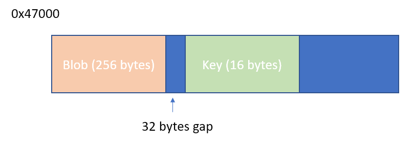
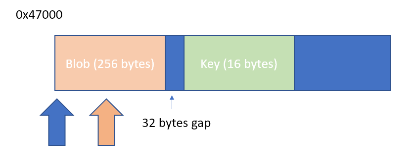
The rest is just patience to trace every input and output of the subroutine to see how each value is generated. After reading things very carefully for a couple of days, I figured out all of the algorithms. It took me another few days to track the key being used, it turns out that the device key is not stored in the SPI flash but in the OTP (one time programmable) area (starting from 0x47000). The blob is broadcasted on the challenge, but the key is not.
The secret recipe (or how to extract your key)
So the code uses some data from the OTP area of the chip for the device encryption key. How can we read this? there are a lot of ways to do it:
Write a new code to read the OTP area
Use a debugger
Patch the existing code
Writing a new code or using JTAG debugger will require me to solder more wires and to get the debugging tools to work. I am trying not to disturb the current soldering that I already made, and I don’t want to setup environment o write a new code, flash it and read the result.
I found a simple way to extract the key by patching a single byte on the firmware. I just shifted the constant that was used to send the blob. Instead of sending only the blob area, it will send also the embedded key that is located 32 bytes after the blob.
Compared to JTAG method, this patch is easier to reproduce by anyone that has a soldering iron and Raspberry Pi or Arduino.
This is just a one-byte patch, by changing the value at 0x6425 (file offset in the decrypted main firmware) from 0x4c to 0x7c, we can extract the device key.
I provided a script to decrypt firmware from SPI flash image, and also another script re-encrypt the decrypted firmware to make a new flashable image. So the steps to get the keys are:
Get the SPI flash content
Extract/decrypt the main firmware
Patch the main firmware (remember to make a backup of the original)
Repack/re-encrypt the patched firtmware
Flash the firmware
Start the PGP
Read the challenge data using any software, the last 16 bytes is the device key
Flash the original firmware
Is there another way to extract the device key? It may be possible to extract it from the memory of the Pokemon Go app while it is running. But even if it is possible now, Niantic may change it so that extraction will not be possible in the future (e.g: by clearing keys after use or even do the decryption on the Niantic server).
Reversing the Pokemon GO game?
I tried reverse engineering the Pokemon GO game, but it is heavily obfuscated. I spent a few hours a day for several days but didn’t get very far. I can explain some of the things that I observed, but I won’t go into much detail since Niantic will probably change them anyway.
Before going deep into the code, I checked on the version history of both the APK and IPA files, hoping that may be in the past they have included the certification process in an unobfuscated form (or less obfuscated form compared to what we have now).
All versions before the release of PGP hardware contains incomplete PGP certification code which is still not obfuscated. Unfortunately, both the iOS and Android version contain obfuscation at the time of the PGP release. The old files are also not easier to read compared to the newer ones.
iOS version of the game
The iOS version consists of a single huge binary named pokemongo. This is a mix of Objective-C, Unity and native C++ code. The binary uses ARM64 code. Due to the size, navigating and extracting something useful from this monolithic binary is quite hard.
There is a group that actively maintains a patched version of Pokemon GO called PokeGO++ (they even have a subscription for this service). They patched the security checks that exist in the binary and added a new library with method swizzling to add new features to the game (such as Teleport, IV Checker, etc). If anyone is interested in reversing the Pokemon GO game, then this would be a good starting point.
I did not investigate the iOS version further, apart from the big binary size, the other reason is that I only have an iPhone 5S which is already too slow to run the Pokemon GO game.
Android version of the game
In the Android version, Niantic employs SafetyNet so that changing the APK will stop it from working. It is also very sensitive to any leftover trace of rooting tools, and the existence of some files will make it refuse to connect.
The Android version consists of Java/Smali Code, Unity code, and native library (accessed through JNI). Using existing tools we can decompile the Java part, but nothing interesting is there. We can also look at names of the Unity classes using existing tools, but the implementation is in native code (not in .NET IL). The native library uses THUMB instruction set instead of ARM/ARM64 (even on 64 bit Android).
Almost every subroutine in the native code is split into tens to hundreds of blocks. My guess is they are using a custom obfuscating compiler, probably a fork of llvm-obfuscator. One subroutine is split into multiple blocks using MOV Rx, PC. This can be fixed using some pattern matching, but after you merged the routines, it turns out that it is still split into multiple small subroutines located far away. This small subroutines only does one thing, for example a+7 or a + b.
Strings are encrypted (obviously), but the decryption is not done in a single place. It is done when needed, and it also uses a different encryption method in each subroutine. So string extraction is not easy.
Although I didn’t implement it, in my opinion, it is possible to unobfuscate a lot of the code. This will require quite a lot of coding. And when you succeed, they will probably already release a new version with a different obfuscation method that breaks your tool.
The native code is accessed using JNI, but it only exports several symbols named java_XXX, for the rest, it uses “registerNativeMethods“. Of course, the address and the name of the methods are obfuscated.
The process for PGP is separate from the game process. The game communicates using SSL. Bypassing the SSL is not too hard, but apart from the initial handshake, subsequent packets are encrypted with custom encryption (they use another layer of encryption on top of SSL).
For the main game process, we can intercept the Unity code to see the request/response in Protobuf form, but unfortunately, this is not possible in the PGP process which is completely native code (it doesn’t load the unity library at all).
During the pairing process, the Pokemon Go game must be connected to the internet. This seems to indicate that whatever process required to generate the key was done on the server (Niantic) side.
Reversing other devices?
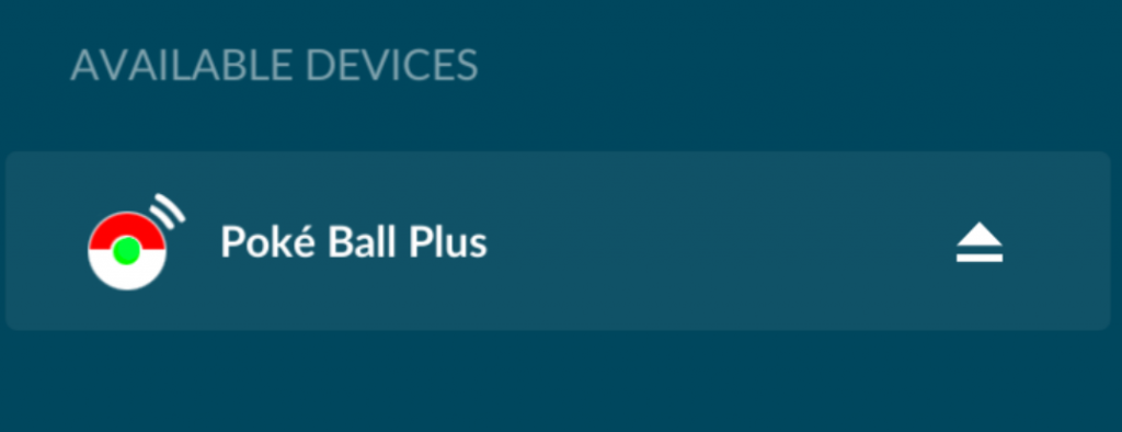
Currently I do not own any other Pokemon GO related devices such as Poke Ball Plus, Nintendo Switch or other implementation of PGP (such as Gotcha, Gotcha Ranger, and Pocket Egg) so I leave it to others to do it, or I might do it when I have the device(s).
One interesting thing is that we can rename the device to Pokemon PBP and it will be recognized and paired as Poke Ball plus.
How can datel/codejunkies and the Chinese do it?
The short answer is I don’t know. I don’t know how they can generate the combination of a new blob, mac address, and device encryption key. Changing a byte in the blob (with same Mac) causes the challenge to be rejected. Changing a byte in the mac address also causes the challenge to be rejected. I only have one device to test and although I have many guesses, I am not sure which one is the answer.
There is a simple formula relating these three, and it doesn’t use any secret key, or
There is an implementation of this algorithm in one of the old version of the game, or
The algorithm was leaked from the PGP factory
Or the explanation could be very different from the one listed above. I am also considering to release my Blob and Key, but I am afraid of these:
Niantic might block this Mac Address from connecting (a bit unlikely, since they seem to allow Gotcha devices with same Mac address, but of course they can always change their mind)
If this mac address is used by many people, everyone will be blocked
I might get sued for publishing the secret key
But for now, I decided to play safe.
If someone wants to sacrifice their PGP and spread the blob/key combination, I suggest to use an original PGP, so that the Mac address is unique. And if that gets banned, you won’t upset a lot of people buying cloned devices.
Please also note Niantic’s stance on this.
Hey Brandon! Pokémon GO Plus is currently the only authorized accessory for Pokémon GO. Using other accessories may negatively affect your gameplay and may result in account blocking or termination. Hope that helps! ^AM
There are several legal things that you can do with the information presented:
You can clone your own device, and make it better (e.g: in a better form factor, with a better display, battery, etc). Cloning your own device for your own use should be undetectable by Niantic.
You can modify the firmware of your PGP (e.g: auto catch or auto spin only)
You can write an app that can communicate with your PGP
Future work
I only played Pokemon GO casually with my family, I am still at level 33 after two years playing this game on and off. Reversing this Pokemon GO Plus is only for fun and to satisfy my curiosity. But I am not that curious to spend a lot of money to acquire other kinds of Pokemon Go related hardware (Gotcha, original Pokemon Go Plus, Poke Ball Plus, etc).
If you want to help me buy other Pokemon GO related hardware or just tip me for this article, you can send it via:
TLDR: If your FL2K dongle only works on USB 2.0 ports, it may have been wired incorrectly. Rewiring it should make it work.
Two weeks ago I learned about osmo-fl2k from Hackaday and immediately ordered one from Aliexpress. Two days ago, I received my order and tested it: it works with USB 2.0 ports on all of my computers (Windows and Linux, Desktop and Laptop), but when I plugged it in on a USB 3.0 port, it is not detected at all.
I verified that the device ID is as expected by osmo-fl2k and that it works (with fl2k-test) on USB 2.0 port although it is very slow (14 MS/s).
The device is never detected on USB 3.0 ports, with or without hubs. No message at all when typing “dmesg”, and Windows also doesn’t show anything on device manager (not even a blink on device manager when the device is plugged in). I verified that all of my USB 3.0 port works by plugging other USB 2.0 and USB 3.0 devices.
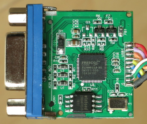
Next step is to open this thing to verify that I really get the correct chip. Fortunately, the chip is correct, although the PCB is a bit different from the one shown in the osmo-fl2k website. The cable soldering seems to be ok, the connection looks good, and they even hot-glue it to make sure it stays that way.
I began to notice that the cabling is a bit different from the one shown in osmo-fl2k website. On the website all 10 cables is on the front side of the PCB, and on mine there are only 8 of them on one side and two on the other side.
I began to suspect something is wrong with the SSTX+/SSTX-/SSRX+/SSRX- cabling. But there is no specification/datasheet for the Chip, so how can I know the correct cabling?
First I tried using my multimeter’s continuity tester to check the color of the cables and the connection. It matches the standard coloring as listed in the USB 3.0 page on Wikipedia. For example, testing D+ pin on the USB port shows that it connects to the green cable and D- connects to the white cable.
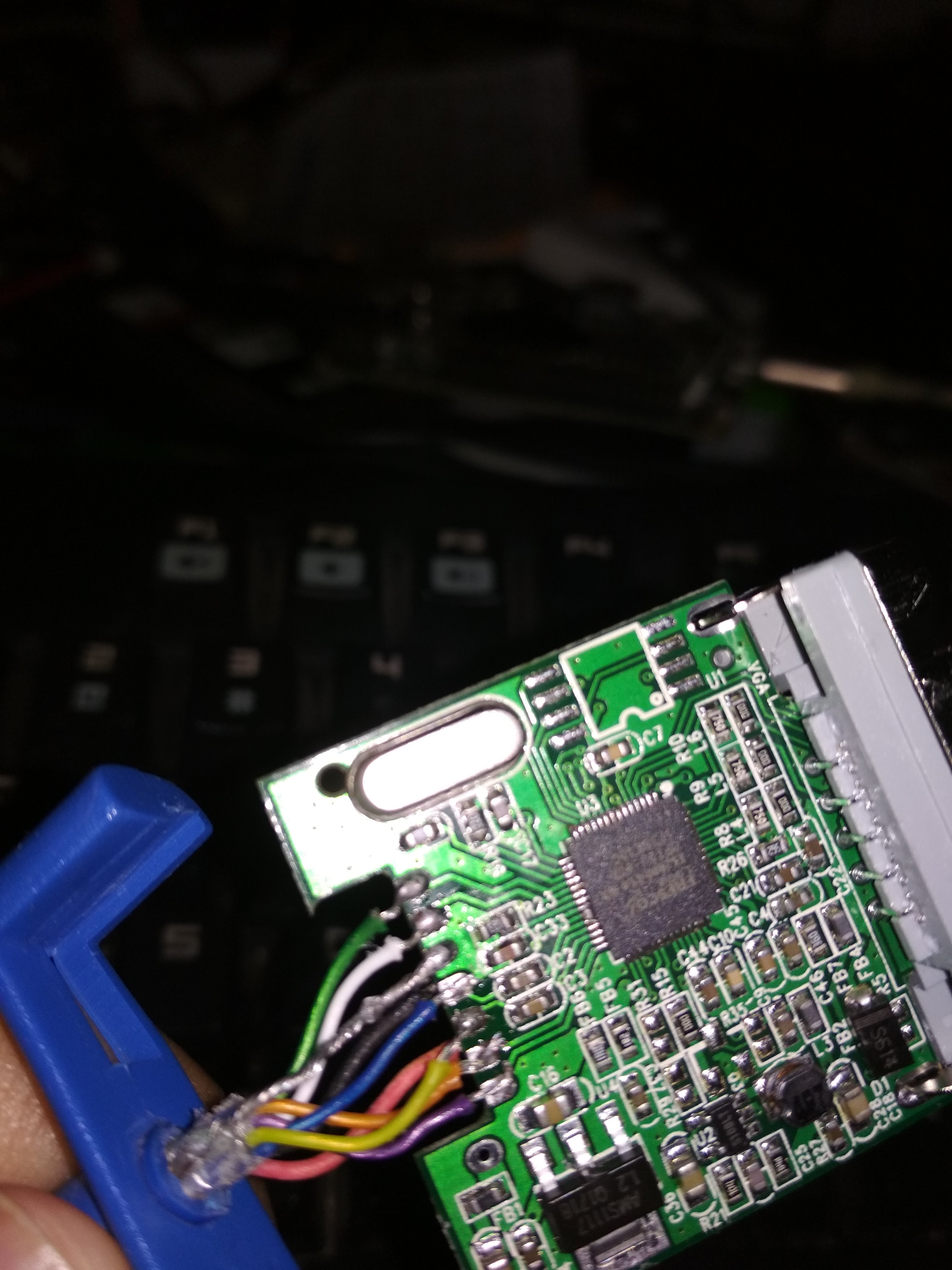
I made an assumption: the quality of dongle used on the FL2K website looks good (mine doesn’t even have the SPI flash chip), so I assume they also use standard colors for the cables. Tracing from the pins to the cable shows that I need to rearrange the cables to match. For example, the first two pins on the top right of the chip should go to purple and orange cables (SuperSpeed receiver differential pair).
Image from osm-fl2k website
After rewiring it, it works fine, the dongle is detected on USB 3.0 ports and I can transmit up to 108MS/s. I have an old motherboard (>5 years), and as you can see from the osmo-fl2k website that the transmission speed depends on the USB 3.0 controller that you have. I have successfully transmitted FM radio signal but I haven’t experimented with other types of signal yet.
After unsoldering and resoldered the cables
So the explanation of why it works on USB 2.0 ports is because it only uses VCC, GND, D+, and D- which was wired correctly. While on USB 3.0 ports, it tried to use the SSTX/SSRX pair and it doesn’t work.
I hope this helps others that have the same problem. Just a word of caution: the colors of your cables might be different from the one that I have, the PCB layout that you receive may also be different, so be careful and double check everything.


 I began to notice that the cabling is a bit different from the one shown in osmo-fl2k website. On the website all 10 cables is on the front side of the PCB, and on mine there are only 8 of them on one side and two on the other side.